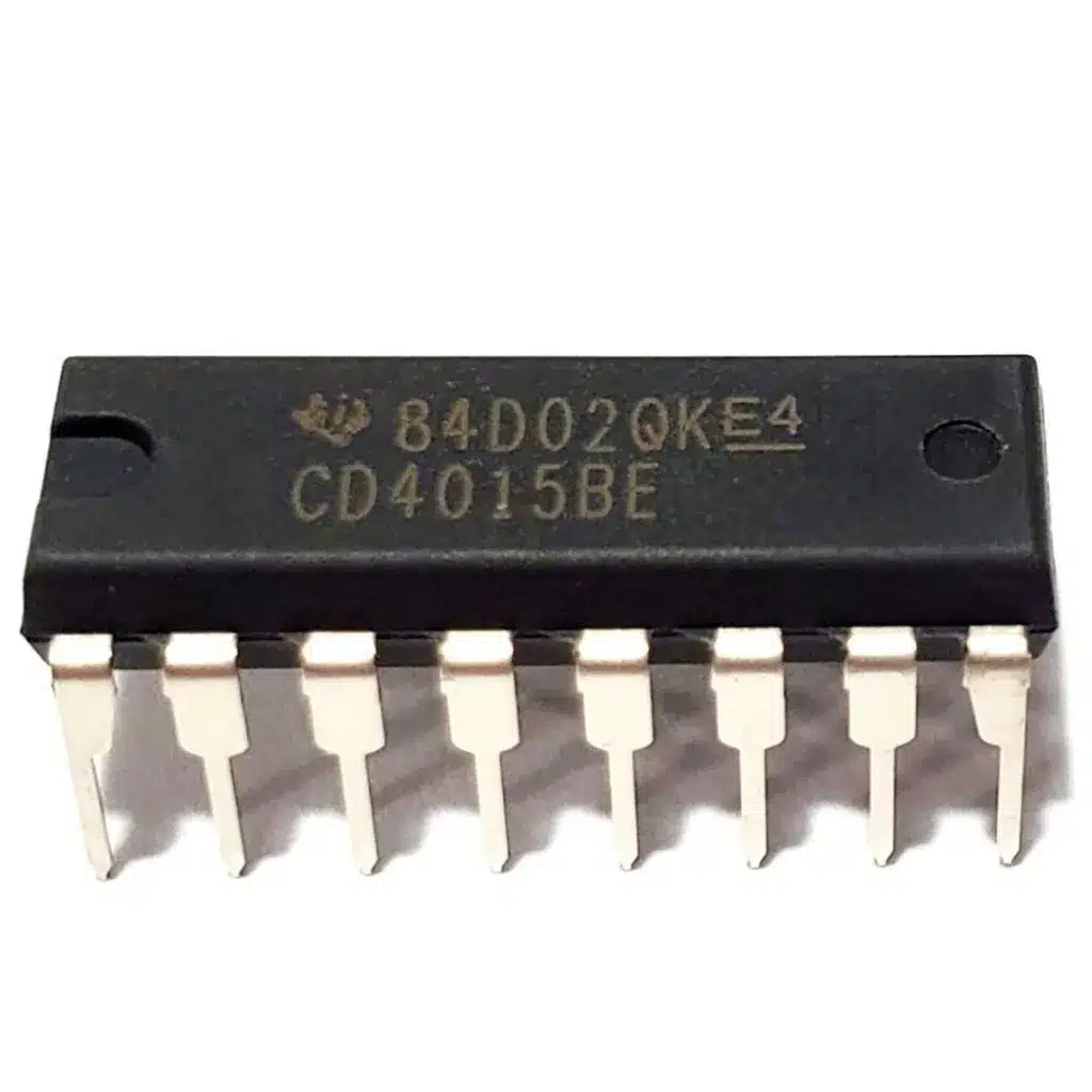
CD4015 Dual 4-Stage Shift Register IC (DIP) Overview
The CD4015 Dual 4-Stage Shift Register IC is a CMOS device that integrates two independent 4-bit shift registers into a single Dual In-line Package (DIP). Each register supports serial data input and parallel outputs, making the IC well suited for digital data storage, transfer, and sequencing tasks in embedded and discrete logic systems.
Key Features of the CD4015 Dual 4-Stage Shift Register
- Two independent 4-bit shift registers in one IC
- Serial input with parallel output for efficient data conversion
- Wide supply range: 3 V to 15 V to match battery or logic rails
- Low-power CMOS technology with high noise immunity
- TTL-compatible input thresholds for easy interfacing
- Standard DIP package — easy to breadboard and solder
Technical Highlights and Specifications
- Function: Dual 4-stage (4-bit) shift registers
- Operating voltage: 3 V to 15 V
- Technology: CMOS — low quiescent current and high noise margin
- Logic compatibility: TTL-compatible inputs
- Package: Dual In-line Package (DIP) for prototyping convenience
- Typical uses: serial-to-parallel conversion, temporary data storage, timing and sequencing
Typical Applications
- Digital counters and data register circuits
- Serial-to-parallel data conversion for displays or parallel buses
- Timing and sequencing circuits in digital systems
- Microcontroller and FPGA interfacing and expansion
- Prototyping, educational projects, and hobby electronics
Why Choose the CD4015 for Your Project
The CD4015 is a versatile and economical choice when you need compact serial-to-parallel capability with wide voltage tolerance. Its CMOS construction offers low power consumption when compared to older bipolar devices, and TTL-compatible inputs simplify connection to many popular logic families and microcontroller I/O.
Integration and Design Notes
- Each of the two registers provides a serial data input and parallel outputs; registers typically share common clock and reset control lines — consult the device datasheet for exact pin assignments and timing diagrams.
- Because the device accepts a wide supply range, decoupling capacitors near the VDD and VSS pins are recommended to maintain stable operation in noisy environments.
- For breadboard prototyping, the DIP package makes wiring and testing straightforward. For production, the device is also available in other package formats (check supplier options).
Note: Images are for Illustration Purposes Only


Reviews
There are no reviews yet