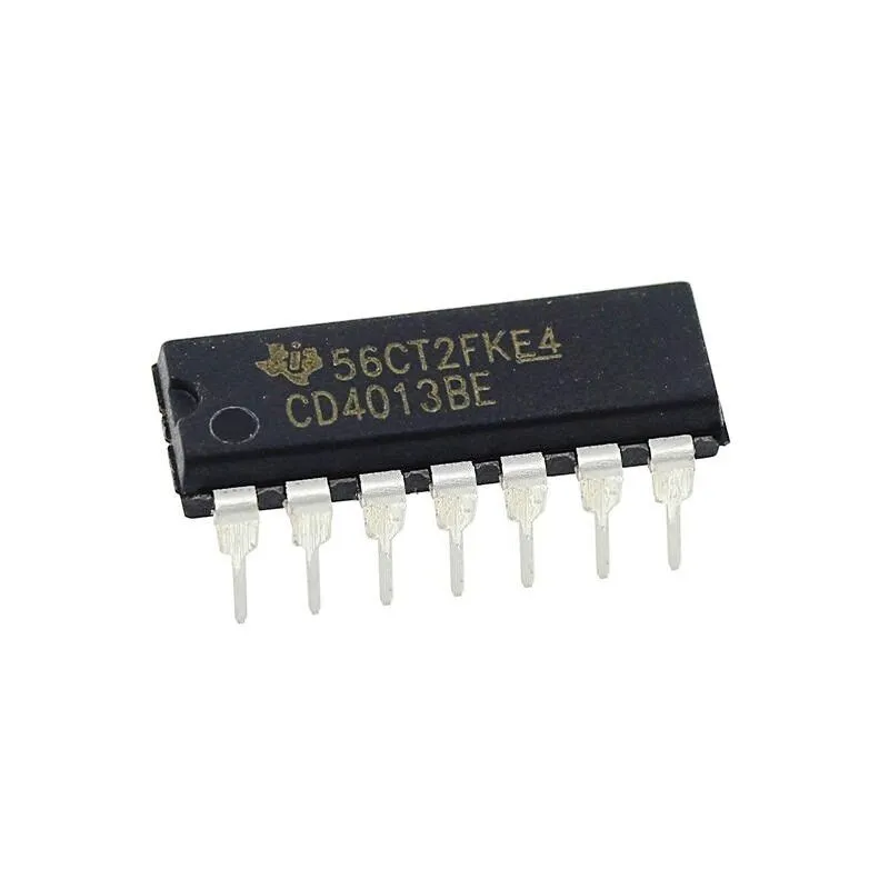
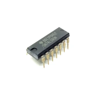
CD4013 Dual D-Type Flip-Flop IC (DIP) — Overview
The CD4013 Dual D-Type Flip-Flop IC is a CMOS logic device that integrates two independent, edge-triggered D-type flip-flops in a single Dual In-line Package. Each flip-flop provides a data (D) input, a clock (CLK) input, asynchronous set (S) and reset (R) inputs, and complementary outputs (Q and Q̅). With a wide operating voltage range and low power consumption, the CD4013 is suitable for hobbyist projects and industrial digital designs.
Key Features
- Two independent, edge-triggered D-type flip-flops
- Complementary outputs: Q and Q̅ for flexible logic arrangements
- Separate asynchronous Set and Reset inputs for each flip-flop
- Wide operating voltage: 3V to 15V
- Low power CMOS technology and high noise immunity
- Standard DIP package for easy prototyping on breadboards and PCBs
Applications
- Frequency division and clock division circuits
- Counters and sequential logic modules
- Data storage, latching, and register functions
- Toggle flip-flop implementations and switch debouncing
- Pulse generation, signal synchronization, and timing circuits
- Shift registers and simple memory elements in digital systems
Technical Specifications
- Logic family: CMOS
- Number of flip-flops: 2 (dual)
- Supply voltage (typical): 3V to 15V
- Inputs: D, CLK, Set (S), Reset (R) per flip-flop
- Outputs: Q and complementary Q̅ per flip-flop
- Package: Standard Dual In-line Package (DIP) for through-hole mounting
Typical Use Cases and Design Tips
- Use as a frequency divider: connect CLK and feed Q back to D for divide-by-2 stages.
- Debounce mechanical switches by using the flip-flop to latch stable transitions.
- Use asynchronous Set and Reset for fast preset or clear of stored state; add pull-up or pull-down resistors as required.
- For microcontroller interfacing, ensure voltage levels match the MCU logic levels when operating at lower supply voltages.
- Place bypass capacitors close to VCC and GND pins to improve noise immunity and stability.
Package and Prototyping
The DIP format of the CD4013 makes it breadboard-friendly and straightforward for prototyping on stripboards or being soldered into through-hole PCBs. Its standard pin spacing simplifies replacement and rapid testing in educational and lab environments.
Why Choose the CD4013 for Your Project
- Flexible: Two independent flip-flops in one IC reduce board space and component count.
- Robust: CMOS process provides low static power consumption and wide voltage tolerance.
- Beginner-friendly: Easy to wire on breadboards and ideal for learning sequential logic design.
Ordering and Notes
Ideal for engineers, students, and hobbyists building counters, registers, timing circuits, or simple state machines. Check datasheets for timing diagrams and electrical characteristics for critical timing and drive requirements.
Note: Images are for illustration purposes only.


Reviews
There are no reviews yet