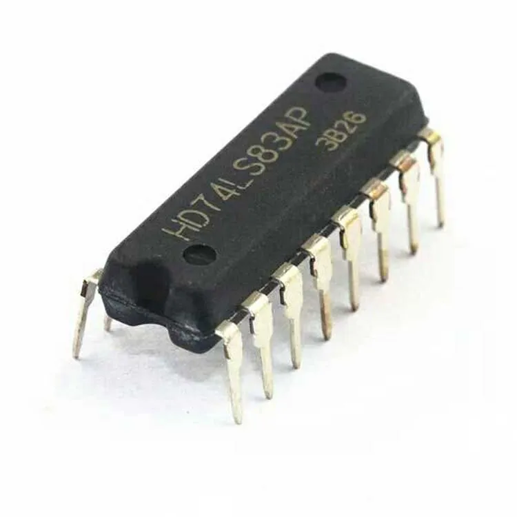
Overview of the 7483 4-Bit Binary Full Adder IC (DIP)
The 7483 4-Bit Binary Full Adder IC is a high-speed TTL device designed to perform binary addition of two 4-bit numbers. The chip integrates four full adder stages in cascade, accepts a carry input (Cin) and produces a carry output (Cout), making it straightforward to build multi-bit adders by cascading multiple ICs.
Features and Specifications
Key Features
- Performs binary addition of two 4-bit numbers (A0-A3 and B0-B3).
- Carry input (Cin) and carry output (Cout) for cascading additional adders.
- High-speed TTL logic for fast arithmetic operations.
- Standard 16-pin Dual In-line Package (DIP) for easy prototyping and PCB mounting.
- Low propagation delay suitable for small ALUs, calculators, and educational projects.
Electrical and Pin Overview
- Logic family: TTL (standard 74xx series behavior).
- Package: 16-pin DIP, breadboard-friendly.
- Typical pins: inputs A0-A3, B0-B3; outputs S0-S3 (sums); Cin (carry in); Cout (carry out); VCC and GND.
Applications
- Arithmetic Logic Units (ALUs) and basic processor arithmetic blocks.
- Digital counters and calculators that require multi-bit addition.
- Microprocessor and computer system design for add/subtract stages.
- Educational digital electronics labs and hobbyist projects.
Typical Use and Cascading Multiple ICs
To build wider adders (for example 8-bit or 16-bit), cascade multiple 7483 ICs by connecting the carry output (Cout) of the least significant block to the carry input (Cin) of the next block. Typical wiring layout:
- Connect A0-A3 and B0-B3 to the respective inputs of the first 7483.
- Use Cin on the least significant IC to set an initial carry (usually 0 for simple addition).
- Connect Cout of the lower-significance IC to Cin of the next IC in the chain.
- Read sums S0-S3 from each IC and the final Cout as the overall carry out.
Package, Mounting, and Prototyping Tips
- 16-pin DIP fits standard breadboards and DIP sockets for quick prototyping.
- Keep VCC and GND decoupled with a 0.1uF ceramic capacitor close to the IC to improve noise immunity.
- Observe proper TTL input voltage levels and avoid floating inputs; tie unused inputs to defined logic levels.
- When cascading, ensure consistent power rails and proper signal routing to minimize propagation delay issues.
Why Choose the 7483 4-Bit Full Adder IC
- Proven TTL design used in countless digital designs and teaching environments.
- Simplifies multi-bit addition with built-in carry propagation.
- Easy to integrate into breadboard experiments, prototype PCBs, and educational kits.
Note: Images are for illustration purposes only.


Anonymous (verified owner) –
Anonymous –