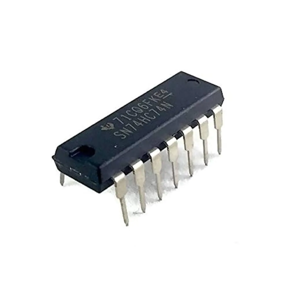
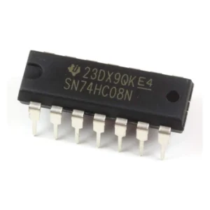
7474 Dual D-Type Flip-Flop IC (DIP) – Product Overview
The 7474 Dual D-Type Flip-Flop IC is a classic TTL 74xx-series device that integrates two independent edge-triggered D-type flip-flops into a single 14-pin DIP package. Each flip-flop captures the logic level present at the D input on the rising edge of the clock and holds that state until the next clock transition. The IC includes asynchronous preset and clear inputs plus complementary outputs for flexible sequential logic design and prototyping.
Key Features
- Two independent edge-triggered D flip-flops in one IC (dual configuration).
- Asynchronous Preset (PR) and Clear (CLR) inputs for forced set and reset (typically active low on standard 74xx variants).
- Complementary outputs: Q and Q9 (true and inverted outputs).
- Captures data on the rising edge of the clock input for synchronous operation.
- Standard TTL operation at +5V supply voltage with fast switching and low propagation delay.
- 14-pin DIP package: breadboard and PCB friendly.
- Easy interfacing with other 74xx family logic devices.
Pinout and Package
The 7474 is supplied in a 14-pin dual in-line package (DIP-14), making it convenient for breadboarding and PCB mounting. Typical pin functions include VCC, GND, two clock inputs, two data inputs, two preset pins, two clear pins, and the two pairs of Q and Q9 outputs.
Electrical and Timing Notes
- Supply voltage: +5V typical for standard TTL operation.
- Edge-triggered operation: data is sampled on the rising edge of the clock.
- Asynchronous preset and clear override the stored state when asserted.
- Low propagation delay and fast switching suitable for clocked digital systems.
Typical Applications
- Data storage elements and small registers.
- Frequency division and counters (divide-by-2 and cascaded configurations).
- Shift register stages and serial-to-parallel or parallel-to-serial conversions.
- State machines, sequencing, and synchronized control logic.
- Debounce circuits, edge detection, and clocked domain transfers.
- Microcontroller and FPGA interfacing in educational and prototyping projects.
Interfacing and Design Tips
- Use proper VCC decoupling (0.1 uF) close to the IC to reduce switching noise.
- When cascading flip-flops for counters or shift registers, ensure clock timing and setup/hold requirements are met to avoid metastability.
- Use PR and CLR to initialize known states at power-up; remember they are typically active low on most 74xx variants.
- Keep signal traces short and avoid long runs for high-speed clock signals to reduce ringing and skew.
Ordering and Notes
- Package: 14-pin DIP (other package options may exist for specific manufacturers).
- Part numbers within the 74xx family may vary by manufacturer and speed grade (for example, 74LS74, 74HC74, etc.). Check the datasheet for the specific variant when timing or power constraints are critical.
Note: Images are for Illustration Purposes Only


Ayesha (verified owner) –
Ayesha –
Anonymous (verified owner) –
Anonymous –
Ali HaMza (verified owner) –
Ali HaMza –